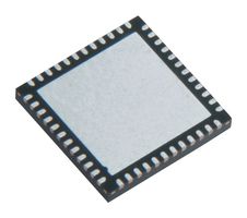
AD9525BCPZ
Clock Generator IC, 3.135 V to 3.465 V, 3.6 GHz, 8 Outputs, LFCSP-48, -40°C to 85°C

| Manufacturer | ANALOG DEVICES |
|---|---|
| Manufacturer Part No | AD9525BCPZCopy |
| Manufacturer Standard Lead Time | 12 weeks |
| Newark Part No. | 54AK0005 |
| Your Part Number | |
| Technical Datasheet |
Need more?
| Quantity | Price |
|---|---|
| 1+ | $28.930 |
| 5+ | $26.130 |
| 10+ | $23.330 |
| 25+ | $22.300 |
| 50+ | $21.260 |
| 100+ | $20.830 |
Product Information
| Manufacturer | ANALOG DEVICES |
|---|---|
| Manufacturer Part No | AD9525BCPZCopy |
| Manufacturer Standard Lead Time | 12 weeks |
| Newark Part No. | 54AK0005 |
| Technical Datasheet | |
| Clock IC Type | Clock Generator |
| Frequency | 3.6GHz |
| Supply Voltage Min | 3.135V |
| Supply Voltage Max | 3.465V |
| IC Case / Package | LFCSP |
| Clock IC Case Style | LFCSP |
| No. of Pins | 48Pins |
| Product Range | - |
| Qualification | - |
| No. of Outputs | 8Outputs |
| Operating Temperature Min | -40°C |
| Operating Temperature Max | 85°C |
| Automotive Qualification Standard | - |
| MSL | MSL 3 - 168 hours |
| SVHC | No SVHC (04-Feb-2026) |
Product Overview
AD9525 is a low jitter clock generator with eight LVPECL outputs. It is designed to support converter clock requirements for long-term evolution (LTE) and multicarrier GSM base station designs. It provides a low power, multioutput, clock distribution function with low jitter performance, along with an on-chip PLL that can be used with an external VCO or VCXO. The VCO input and eight LVPECL outputs can operate upto a frequency of 3.6GHz. All outputs share a common divider that can provide a division of 1 to 6. It offers a dedicated output that can be used to provide a programmable signal for resetting or synchronizing a data converter. The output signal is activated by a SPI write. It is used in applications such as LTE and multicarrier GSM base stations, clocking high speed ADCs, DACs, ATE and high performance instrumentation, 40/100Gb/sec OTN line side clocking, cable/DOCSIS CMTS clocking, test and measurement.
- Integrated ultralow noise synthesizer
- 8 differential 3.6GHz LVPECL outputs and 1 LVPECL SYNC output or 2 CMOS SYNC outputs
- 2 differential reference inputs and 1 single-ended reference input
- Input sensitivity is 200mV p-p typical at (frequency at 122.88MHz)
- Input frequency range from 0MHz to 500MHz
- Rise time/fall time (20% to 80%) is 105ps typical
- Operating temperature range from -40°C to +85°C
- Package style is 48-lead lead frame chip scale (LFCSP-WQ)
Notes
ADI products are only authorized (and sold) for use by the customer and are not to be resold or otherwise passed on to any third party
Technical Specifications
| Clock IC Type | Clock Generator |
|---|---|
| Supply Voltage Min | 3.135V |
| IC Case / Package | LFCSP |
| No. of Pins | 48Pins |
| Qualification | - |
| Operating Temperature Min | -40°C |
| Automotive Qualification Standard | - |
| SVHC | No SVHC (04-Feb-2026) |
| Frequency | 3.6GHz |
|---|---|
| Supply Voltage Max | 3.465V |
| Clock IC Case Style | LFCSP |
| Product Range | - |
| No. of Outputs | 8Outputs |
| Operating Temperature Max | 85°C |
| MSL | MSL 3 - 168 hours |
Technical Docs (3)
Legislation and Environmental
| US ECCN: | EAR99 |
|---|---|
| EU ECCN: | Unknown |
| RoHS Compliant: | Yes RoHS |
| RoHS Phthalates Compliant: | Yes RoHS |
| SVHC: | No SVHC (04-Feb-2026) |
| Download Product Compliance Certificate | Product Compliance Certificate |