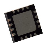
MAX5550ETE+
DAC, 10BIT, DUAL, TQFN-16

Need more?
| Quantity | Price |
|---|---|
| 1+ | $7.040 |
| 10+ | $5.460 |
| 25+ | $5.060 |
| 50+ | $4.840 |
| 100+ | $4.620 |
| 300+ | $4.550 |
| 500+ | $4.480 |
Product Information
Product Overview
The MAX5550ETE+ is a dual, 10bit, programmable, high output current digital to analogue converter (DAC) in 16 pin TQFN package. It sources up to 30mA per DAC which makes it ideal for PIN diode biasing applications. Outputs can also be paralleled for high current applications (up to 60mA). The MAX5550 typically consumes 1.5mA per DAC in normal operation and less than 1μA in shutdown mode while operating from single 2.7V to 5.25V supply. The device also has low output leakage current in shutdown mode (±1μA maximum) that is essential to ensure that the external PIN diodes are off. A separate reference input (REFIN) allows for use of an external reference source such as MAX6126 for improved gain accuracy. A pin selectable I2C/SPI compatible serial interface provides optimum flexibility for MAX5550. The maximum programmable output current value is set using software and an adjustment resistor. It is used in PIN diode biasing, RF attenuator control and VCO tuning.
- Supply current of 3mA (VDD = +5.25V, no load) and shutdown current of 1.2μA
- Operating temperature range from -40°C to 85°C
- Offset of -16LSB, zero scale error of 1μA and full scale error of -16LSB
- Monotonic over extended temperature range
- Dual outputs for balanced systems
- Integral nonlinearity (INL) of ±2LSB and differential nonlinearity of ±1LSB (monotonic)
- Output stable with RF filters and internal or external reference capability
- Integrated 1.25V bandgap reference & control amplifier for high accuracy & low noise performance
- Digital output (DOUT) available for daisy chaining in SPI mode
- Programmable output current range set by software and adjustment resistor
Applications
Signal Processing
Notes
ADI products are only authorized (and sold) for use by the customer and are not to be resold or otherwise passed on to any third party
Technical Specifications
10bit
I2C, SPI
2.7V to 5.25V
16Pins
-40°C
-
MSL 1 - Unlimited
-
2.7V to 5.25V
TQFN
Serial
85°C
-
No SVHC (25-Jun-2025)
Technical Docs (1)
Associated Products
3 Products Found
Legislation and Environmental
RoHS
RoHS
Product Compliance Certificate